Logic Design for Array-Based Circuits
by Donnamaie E. White
- Table of Contents
- Preface
- Overview
- Chapter 1 Introduction
- Chapter 2 Structured Design Methodology
- Chapter 3 Sizing the Design
- Chapter 3 Appendix = Case Study in Sizing a Design
- Chapter 4 Design Optimization
- Chapter 5 Timing Analysis for Arrays
- Chapter 6 External Set-up and Hold Times
- Chapter 7 Power Considerations
- Case Study: DC Power Computation
- Case Study: AC Power Computation
- Chapter 8 Simulation
- Case Study: Simulation
- Chapter 9 Faults and Fault Detection
- Chapter 10 Design Submission
- ASIC Glossary
Introduction
Semi-Custom Arrays
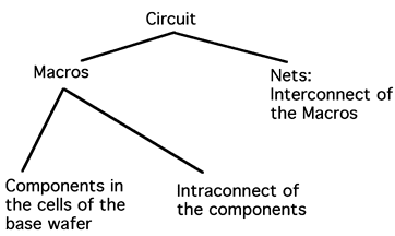
A compromise between off-the-shelf modules and full custom semiconductors is semi-custom design. Semi-custom combines a manufacturerdesigned base wafer with all components in place (resistors, diodes, transistors, etc.) and a customer-generated interconnect pattern to implement the desired circuit. (Refer to Figure 1-2.)
A SEMI-CUSTOM ARRAY CONSISTS OF:
-
Base wafer
-
Macro Intra-connects
-
Placement
-
Interconnects
The interconnect pattern, also called a netlist, is generated from the customer-designed schematic and restricted to the topmost mask layers. Most arrays require two metal layers and a via (through hole) mask layer. Some arrays require three metal and two via layers. Three-layer arrays may use two layers for global interconnect and the third for macro intraconnect, but there are no hard rules.
The more layers, the more prototype debug time required. This may be compromised with the significant gain in power management possible with the third layer.
The schematic for a semi-custom array-based circuit is built up from a library of macros released library that represent SSI, MSI, and sometimes LSI functions. If a different macro is needed from those in a released library, the manufacturer, for a fee, can usually generate a special custom macro (cell and component dependent). Most manufacturers prefer that the released macros be used.
Figure 1-2 Circuit Composition
Semi-custom arrays allow a designer to create at the SSI-MSI level, with familiar functions, without a detailed knowledge of the underlying technology. Semi-custom arrays may themselves contain elements of bit-slice components, allowing both the hardware and the software to be tailored to the application. For example, at least one CMOS array uses the AMD Am2909 sequencer as a macro.
If the designer is experienced and familiar with the macro library, the resulting silicon usage may approach that required by the best full custom design.
CBA (cell-based arrays) and the now more-popular standard-cell libraries [popular as of 1999] are macro collections. The differences between them involve how they are built in the sub-strata of the base die. CBA designs led the size war for some time; standard cells now produce typically smaller die sizes. Approximate estimates were for 10,000 array-starts in 2000; spilt 50-50 between these two technologies, the first time standard cells had come on so strong.
Metalization layers are the customizable layers in a semi-custom array. Metalization, which sits on top of the base die, currently runs to 6 layers, 4 for interconnect and 2 for power-ground, although this may vary. The number of layers of metalization is expected to increase. Keep in mind that between each routing metalization layer, is a layer of vias, the vertical interconnects.
Simple Semi-custom Devices
At the simplest end of the semi-custom spectrum are gate arrays, providing one level of interconnect to the user for specification with all other connections defined.
Programmable devices such as PLAs (programmable logic array), PALs (programmable array logic), field-programmable muxs, sequencers, gate arrays, and other modules are available for limited quantity applications. (PLAs allow both AND and OR gates to be programmed PALs allow only the AND gates to be programmed.) Programmable devices are restrictive in the functionality provided. They are suitable and competitive when there is a match between a module and the current application.
Field-programmable devices are to VLSI what the ROM/PROM is to the microprocessor, i.e., they support and enhance the design project. These devices provide board-clean-up functions, incorporating the simple functions that do not fit into a full semi-custom array or that were found necessary to augment in a bit-slice or fixed instruction set design.
They are still with us.
Copyright © 1996, 2001, 2002, 2008 Donnamaie E. White , WhitePubs
Enterprises, Inc.
For problems or questions on these pages, contact [email protected]