Logic Design for Array-Based Circuits
by Donnamaie E. White
Copyright © 1996, 2001, 2002, 2008, 2016 Donnamaie E. White , WhitePubs Enterprises, Inc.
- Table of Contents
- Preface
- Overview
- Chapter 1 Introduction
- Chapter 2 Structured Design Methodology
- Chapter 3 Sizing the Design
- Chapter 3 Appendix = Case Study in Sizing a Design
- Chapter 4 Design Optimization
- Chapter 5 Timing Analysis for Arrays
- Chapter 6 External Set-up and Hold Times
- Chapter 7 Power Considerations
- Case Study: DC Power Computation
- Case Study: AC Power Computation
- Chapter 8 Simulation
- Case Study: Simulation
- Chapter 9 Faults and
Fault Detection
- Introduction
- Controllability
- Observability
- Masking a Fault
- Fault Types
- Fault Equivalencies
- Single Stuck-At Faults
- Minimal Test Sets
- Example Test Set
- The Problem
- Combinatorial Circuit
- Formation Rules for the Existence Function
- Forming Links
- Selecting a Chain
- Advantages of the Test Sequence
- Simple Gates - Sequences
- Extension to Three-State and Bidirectional Structures
- Extension to Sequential Circuits
- Reference
- Case Study - 16:1 MUX D Flip/Flop Circuit
- Chapter 10 Design Submission
- ASIC Glossary
Faults and Fault Detection
Last Edit July 22, 2001
Case Study - 16:1 MUX D Flip/Flop Circuit
100% FAULT-GRADE VECTOR SET
The following circuit was developed as a teaching circuit and as such has parameters and labels beyond what would appear in an actual circuit schematic. These parameters have nothing to do with the required Functional, AC Test or Parametric Vector sets.
A parametric gate-tree, used for VIH and VIL measurement is included and its output signal is listed. A simulation format requires that all I/O signals and internal enable nets be listed.
The test sequence for a 16:1 MUX 'was altered to allow clocking to occur between vector steps. The rule of one input per vector changing state is honored in that data and clock do not change in the same vector. The sequence begins after the circuit RESET is executed.
Both the schematic set and a formatted (compacted) output vector set is shown here. The output vectors include input, output and enable signals.
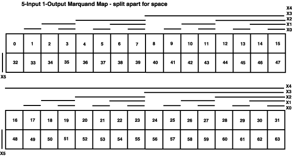
The Marquand Map
The Marquand Map for logical analysis was proposed in a mathematical paper in the late 1800's. It is a convenient mapping method for large functions. The Karnough Map was developed in the 1950's specifically for 4-variable circuits (for coding) and is messier to use in these cases. Figure 9-10 through Figure 9-13 show different sizes of Marquand Maps with minterms labeled.
Figure 9-10 2-Input 1-Output Marquand Map
![]()
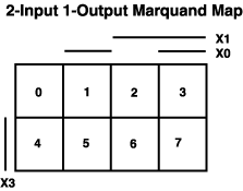
Figure 9-11 3-Input 1-Output Marquand Map
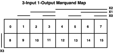
Figure 9-12 4-Input 1-Output Marquand Map
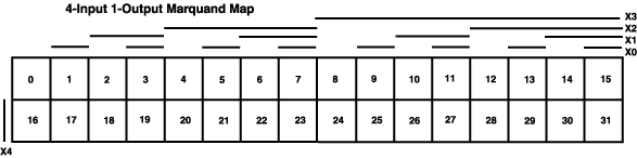
Figure 9-13 5-Input 1-Output Marquand Map (Split)
Copyright © 1996, 2001, 2002, 2008, 2016 Donnamaie E. White , WhitePubs
Enterprises, Inc.
For problems or questions on these pages, contact [email protected]