Tying the System Together
Last Edit November 1, 1996; July 20, 2001
The two basic building blocks of a general 16-bit system -- the
CCU, including the firmware interrupt controller, and the RALU
-- have been defined in previous chapters. Various other devices
are available in the Am2900 family to complete the basic CPU that
has been used throughout the text.
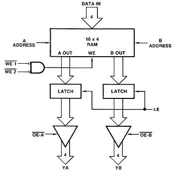
Expanded Memory for the Am2903
The Am2903 is designed to be interconnected to the Am29705, via
decoders, in order to expand the basic 16x4 scratchpad memory. The
Am29705 is a true two-port 16x4 RAM memory which can operate identically
to the Am2903's own scratchpad. A logic diagram of the Am29705 is
given in Figure 7-1. (The Am29203 uses the Am29707 version.)
Figure 7-1 Am29705 block diagram
By expanding the A, B addresses, scratchpad memory
may be added in increments of 16 registers of the equivalent width
of the ALU. An expanded memory interconnect diagram is shown in
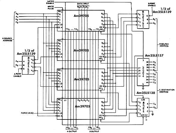
Figure 7-2 (taken from the original AMD data sheet).
Figure 7-2 Three-Address 64 by 4 memory. A 64-word
by 4-bit three-address memory. Data is read from the A address to
the YA outputs and from the B address to the YB outputs while the
latch enable is HIGH. When the latch enable goes LOW, the YA and
YB data are help in the internal latches, and the RAMB address is
switched to the C destination address lines. A write pulse will
then deposit the input data into the location by the C address.
MUX Requirements
In the course of examining the various arithmetic and shifting
algorithms that any given system is to perform, including those
few examined in this text, the designer will find it necessary to
be able to vary
- the way that the RALU RAM and Q shifters interconnect
- the value of carry-in
- the source of the carry out status bit
The carry in bit could be
- from a field in the CCU
- from the ALU Cout (for rotate-by-add or for multiple word precision
algorithms)
- from the ALU Z status line (for the Am2903 multiply for example)
The carry out bit could be sourced from
- the Cn+4 of the RALU
- the RAM3 (or S3) output of the RAM shifter.
The shift and rotate interconnections are determined by the particular
variations which any given design is to implement. RAM0 (Am2901)
or S0 (Am2903) might require connection to Cout, RAM3 (S3), Q3 (extension
register shifter), and ground, VCC or both. Q0 might require a similar
flexibility of connection. RAM3 (S3) and Q3 would require complementary
connection capability.
In each of these cases, the most obvious solution has been to employ
multiplexors with the microinstruction supplying the appropriate
selection for any desired connectivity pattern. The Am2904 is designed
to replace the carry-in MUX, the carry-out MUX, the RAM0 and RAM3
MUXs, and the Q0 and Q3 MUXs. The Am2904 was developed to reduce
the required SSI and MSI support (a.k.a. glue logic) which occurs
in typical CPU designs.
Status Register
In the preferred architecture, the one being emphasized throughout
this text, a status register is used to hold the status produced
by the previous microinstruction (such as the ALU status outputs)
for use in determining the next microinstruction address ("branch
on result of previous"). The status outputs of the RALU as well
as certain other conditional MUX inputs are considered to be microlevel
status inputs.
A sophisticated architecture may also have machine-level status
lines, those bits to be tested by the machine-level instructions.
A machine-level status register is necessary in this case, and it
must be settable at the individual bit level. The Am2904 includes
both the microlevel and the macro or machine-level status registers
and provides the bit set and certain testing capabilities to further
reduce the SSI-MSI system logic support required.
|